
Market Analysis: Advanced Copper Interconnect Chemistry and Management Update
2025-2030 TAM Growth Drivers and The Chosen One (Stock) Dominates.

For my non-paying subscribers, the paywall initiates just before the meat of the content- Table of contents item 5- Meeting with management. They have provided us with some valuable information that updates our thesis, and gives us relevant information as to where we need to pose our next questions for when we meet with them again.
Table of contents
Executive summary
TAM map: advanced copper interconnect chemistry (2025–2030)
PCB: HDI microvia fill + fine-line (mSAP/SLP)
Packaging (PKG): RDL, Cu pillars, TSV
Semiconductor: hybrid bonding + TGV (early-stage)
Management update (paywalled)
What changes vs. the original thesis
What was reinforced about business quality
What it means for the thesis
Disclosure & disclaimer
Appendix: sources used for TAM charts
Thank you
I am grateful to my paying subscribers, who enable me to do this work. Quick note before we start: I’m trying to keep this Substack high-signal. I’d rather publish less often and only when there’s genuinely new, decision-useful research to share. If you have preferences on format or frequency after reading this post, message me, this is funded by you, and I’ll adapt.
Executive Summary
Advanced copper interconnect chemistry is a small, high-ASP (average selling price), oligopolistic niche. Each layer of the stack, PCB, PKG, and Semiconductor, has a different growth and moat profile.
However, most of the money (medium-term) will be made in high-end PCBs where HDI Microvia Fill, and Fine-Line Pattern (mSAP), the chemical processes which are used in tandem, lead the growth.
The electronic consumer industry is at the forefront of this demand, with smartphones and their high-end PCBs, at the helm.
Guess who dominates that market? You guessed it… yours truly- The Chosen Stock.
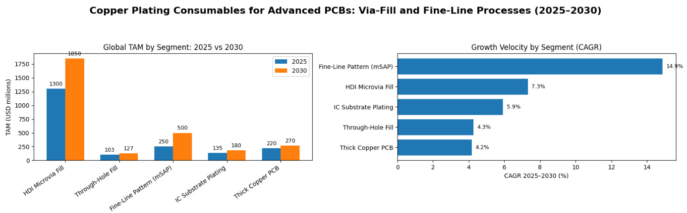
An overview of the TAM for advanced copper interconnect chemistry (via-fill + fine-line + packaging interconnects).
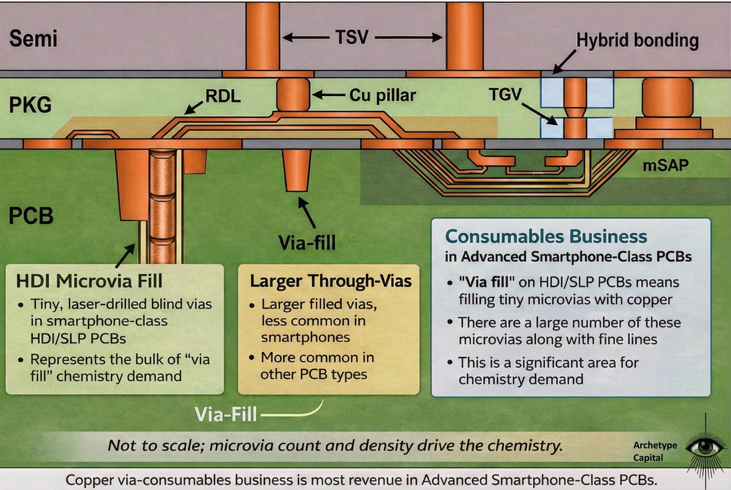
Advanced copper interconnect chemistry is a niche, high-ASP consumables market spanning PCB microvia fill + fine-line patterning, plus advanced packaging interconnects (RDL, Cu pillars, TSV, and eventually hybrid bonding / TGV). Suppliers exist in an oligopoly and tend to be concentrated in the highest-spec processes, and growth is driven by tighter interconnect requirements across smartphones, AI infrastructure, and advanced packaging.
To make it simple, we are looking at three layers of the stack.
PCB (Printed circuit board)- The big green slab.
PKG- The middle green slab.
Semiconductor- The top grey slab.
PCB (Printed Circuit Board): Think of this as the foundation. It is the sturdy baseboard that physically holds the entire system together and connects the memory (RAM), USBs(ports), power, storage (SSD).
PKG (Package Substrate): Think of this as the Brain Stem / Translator. The Chip speaks a language of "nanometers" (microscopic), while the PCB speaks "millimeters" (visible to the eye). You cannot connect them directly; it would be like trying to plug a lightning cable into a wall outlet without an adapter. The PKG translates the Chip’s microscopic, fragile signals into a larger, tougher format that the clumsy PCB can actually grab onto.
Semiconductor (The Chip/Die): Resting on the very top, this is the brain. It is the actual silicon slice where all the computing happens, but it is too fragile and intricate to touch the main circuit board directly without the PKG bridge beneath it.
Within the stack, you can see the copper interconnects.
We’re going to focus on the copper plating consumables market, starting at the PCB layer (microvia fill + fine-line).
PCB (Printed circuit board)- The big green slab.
The image below is my best attempt to conduct a market analysis on the TAM for the chemistry that goes into PCB, and PKG - the TWO green slabs, specifically.
Use the chart as a map: the PCB profit pool is dominated by two things — (1) vertical connectivity (HDI microvia fill) and (2) horizontal wiring density (fine-line patterning via mSAP, often inside SLP boards). Everything else is smaller today, even if some categories are growing fast.
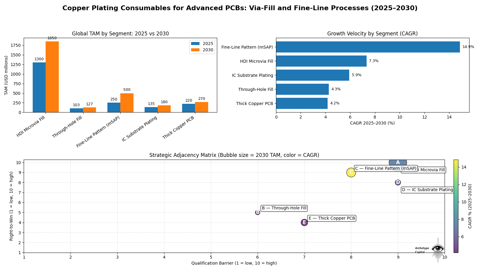
Most modern smartphones use HDI (laser-drilled microvias + build-up layers). The highest-end smartphones use SLP, which is still HDI, but with much finer wiring and is typically enabled by mSAP (Modified Semi-Additive Process- it is a manufacturing technique).
1. HDI (High Density Interconnect)
What it is: The standard for modern smartphones and laptops for the last decade.
The Tech: Unlike old-school green circuit boards, HDI uses “Microvias” (tiny laser-drilled holes) to connect different layers of the board. This allows components to be packed tighter together.
The Process: Circuit formation is often subtractive, but real boards can mix approaches by layer depending on cost/yield/design targets.
2. SLP (Substrate-like Board). (Fine-Line Pattern mSAP).
SLP is best described as an ultra-high-density form of HDI that moves PCB manufacturing toward package-substrate-like feature sizes and process control.
What it is: The “Ferrari” of motherboards (or main logic board for you technical guys). It is the next evolution after HDI, used in flagship devices, like the latest iPhones, Samsungs.
Why “Substrate-like”? It is still technically a motherboard (PBC), but it is built using techniques borrowed from semiconductor packaging (IC Substrates). It bridges the gap between a chip and a board.
The Tech: It allows for materially finer line width/line spacing (often enabled by mSAP). This shrinks the board size dramatically, leaving more room inside the phone for a bigger battery.
Following the money, HDI Microvia fill and Fine-Line Pattern mSAP (SLP) are where we should keep our focus on. SLP sits on the advanced end of the HDI continuum.
The chemicals for HDI/SLP’s biggest market is mainly smartphone PCBs, but growth is also spurting out in nascent industries that, over time, will add a considerable amount of TAM to this market:
Self-Driving cars.
VR Headsets.
Data centers (this is specifically regarding PCB boards, not PKG substrates)
This is an industry that is positioned to grow however which way you look. I didn’t add smartphones here because it would dwarf the categories below and make the chart look a bit silly (as shown after).
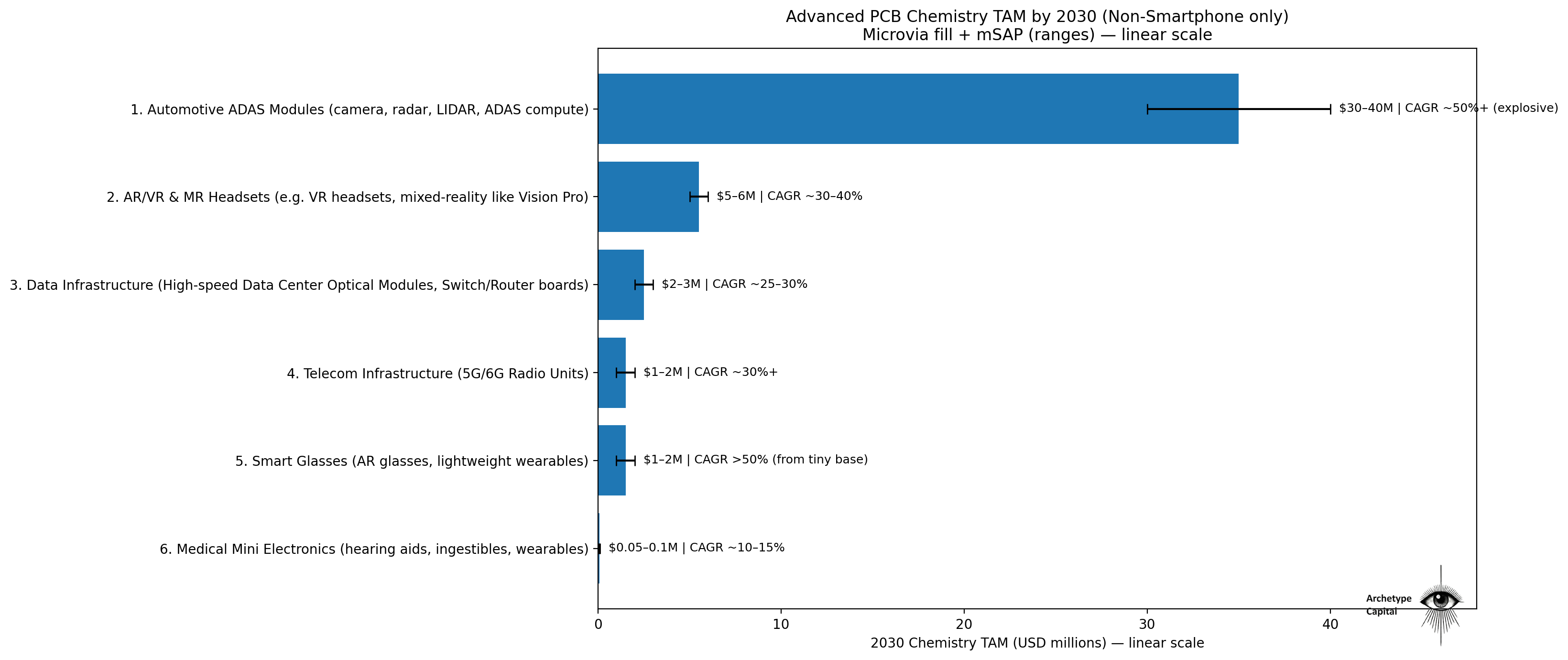
Smartphones currently dominate this market.
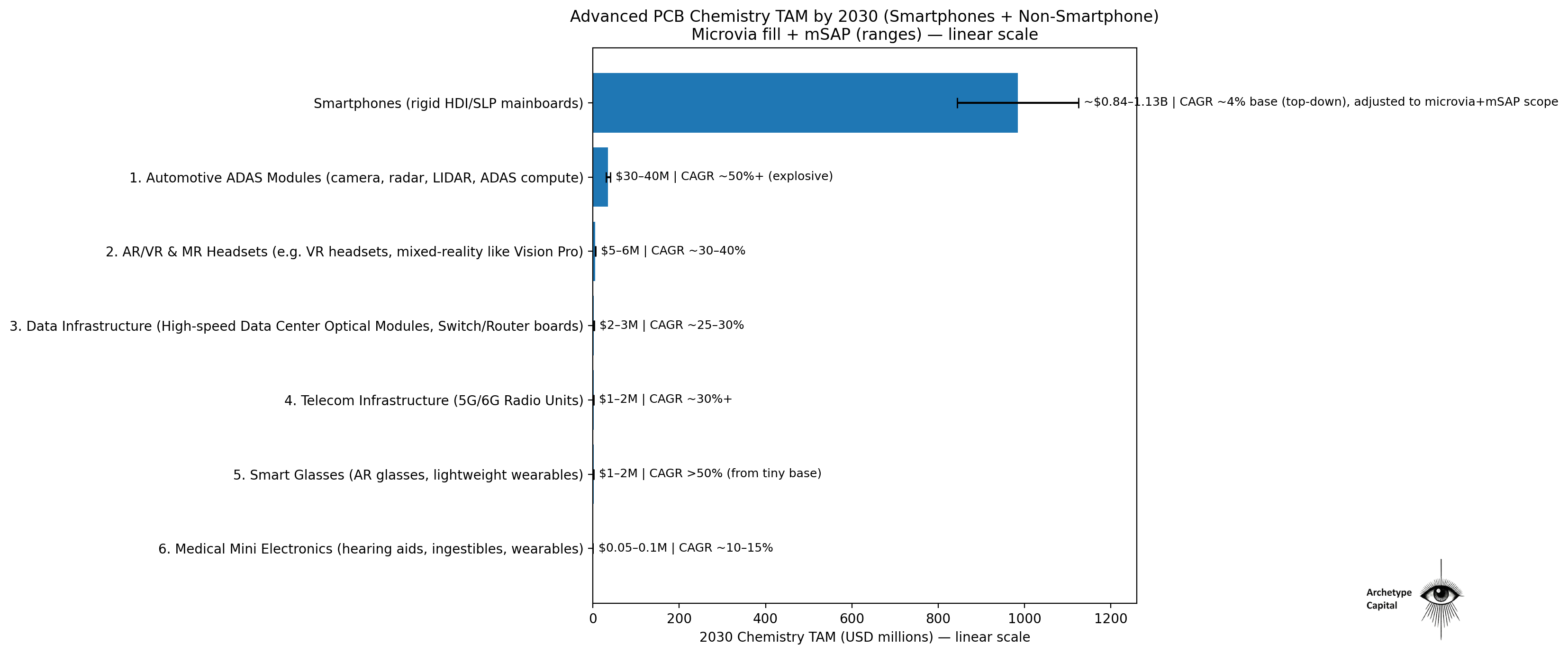
The takeaway here is that via filling for high-end (PCBs) for smartphones lead the nominal growth in the advanced copper interconnect chemistry market, but other industries, like automotive ADAS modules and VR/AR, are growing at such a rapid clip (30-50% CAGR) that they are bound to eventually contribute meaningfully to via filling too. There are other nascent industries like advanced robotics, which will, over the long-term, significantly contribute too.
PKG- The middle green slab
The PKG Substrate is where things get more advanced. I do not know different ASP (average selling prices) yet.
The largest advanced packaging interconnect chemistry pools today include RDL and Cu pillar plating; TSV (Through Silicon Via) is the main ‘via’ analogue at the package level.
The PKG substrate is where interconnect chemistry gets more specialized. Here, the big consumables pools are less “via filling” and more advanced interconnect plating, especially RDL (fan-out / redistribution wiring) and Cu pillars (bump replacement for performance packages). TSV is the closest analogue to true via-fill at this layer.
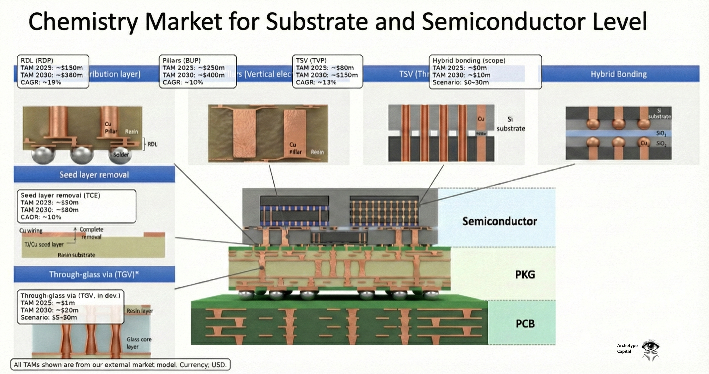
Note* this is a different chart, it is the analysis of the chemistry market for the PKG-Semi layer
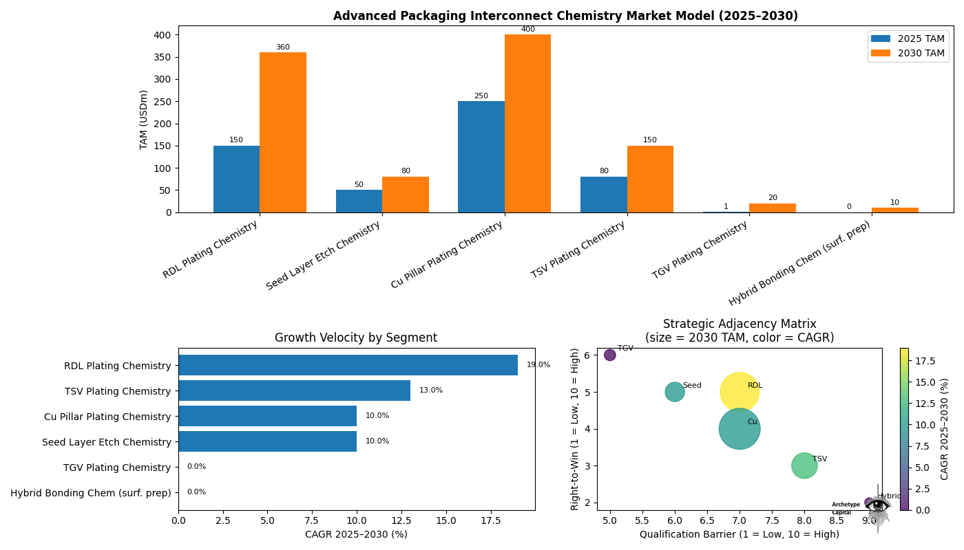
*Note: for TGV and hybrid bonding, CAGR is shown as “0%.” (not meaningful) because the markets are too early-stage for clean growth math off a small/zero baseline.
RDL (Redistribution Layer):
TAM (~$150M, CAGR 19% est 2025- 2030)
Status: Common Practice.
Context: This is widely used in “Fan-Out” packaging (used in smartphones and processors). While the technology is established, the industry is pushing for “finer” RDL (smaller lines), which keeps the chemical requirements high.
Pillars (Cu Pillar):
TAM (~$250M, CAGR 13% est 2025- 2030)
Status: Standard.
Context: These have largely replaced older “solder bumps” (C4 bumps) for performance chips. They are the workhorse connection for the last decade of processors.
Semiconductor Level
Hybrid Bonding:
TAM - Yet to be seen. Average selling prices will probably be high, but undetermined as of now.
Status: New / Ramping Up.
Context: This is the “next big leap.” It abandons solder bumps entirely to fuse chips directly (copper-to-copper). It is currently used in high-end 3D stacking (like AMD’s 3D V-Cache) and is the future for “stacking” logic and memory. In the “Advanced Packaging Interconnect Chemistry Market Model” Below TAM is very low- but only because there is very little information out right now- its too new commercially.
Through-Glass Via (TGV):
TAM - Yet to be seen. Average selling prices will probably be high, but undetermined as of now.
Status: Emerging / In Development.
Context: This is the most “futuristic” item on the chart. Glass substrates are being developed to replace current resin/organic substrates because they are stiffer and handle heat/signals better. Intel, and others are targeting this for ~2026–2030. It is largely pre-commercial for mass logic production.
Putting it together: the medium-term profit pool for advanced chemistries is concentrated in advanced PCB workflows (HDI to SLP/mSAP), while the packaging and semiconductor layer adds longer-dated optionality (RDL, pillars, TSV, and eventually TGV/hybrid bonding).
With that context, the key question is simple: how much of the “cash engine” does The Chosen One control today, and what does management’s latest commentary change in our original thesis?
I think you will be pleasantly surprised. Let’s dive in.